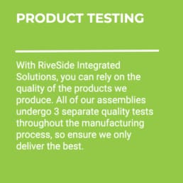
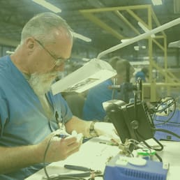
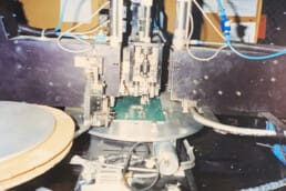
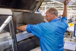
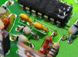
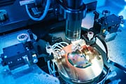
The printed circuit board (PCB) is at the heart of every electronic device. We interact with PCBs numerous times throughout our day. From laptops and cell phones to smart TVs and refrigerators; they’re everywhere! However, most people do not fully understand what a PCB actually is or how it works. In the simplest form, PCBs consist of sheets of non-conductive substrate overlaid with circuitry. This circuitry is typically copper and provides the necessary conductivity. Typical substrate materials include fiberglass and polyester. Electronic components, such as resistors, transformers, transmitters and capacitors, are connected to the board. To form a functional circuit, traces connect the various components to the overlaid circuitry. As technologies advance, PCBs shrink in size but grow in capability. This is due mainly to the demand for more portability and higher functionality. The popularity of hand-held and wearable devices for consumer and commercial markets is largely pushing this trend. High-density circuitry is an amazing advancement that has enabled smaller, more tightly packed boards for these devices. PCB assembly (PCBA) providers must keep up with rapid advancements. This means being able to assemble smaller, more complex panels without sacrificing quality. To help with this, many original equipment manufacturers (OEMs) outsource their PCBA to a reliable contract manufacturer. When selecting a PCBA supplier, OEMs must choose a partner, like Riverside Integrated Solutions (RIS), that employs advanced technologies. At RIS, we focus on meeting the challenges that PCB innovations present at every turn. Below are the ins and outs of the latest in PCBs and PCBA technologies. There are several different types of assembled PCBs. The type is selected based on the application of the electronic device. This factors in the desired functionality, complexity and spatial limitations. Below are some common forms of PCBs. These are the least complex and are easiest to manufacture. The boards have a single layer of conductive material and only occupy one side of the substrate. As the name suggests, this type has conductive material on the top and bottom of the substrate. This type denotes a board with more than two conductive layers. Multi-layer PCBs are often 4-, 6-, or 8-layer panels. OEMs utilize these in more complex electronics applications. PCB designers must also determine the level of flexibility in the printed circuit board. Traditional PCBs are rigid and inflexible, but flexible PCBs are gaining popularity. Flexible PCBs, categorized as flex, have more bend and can withstand more movement than traditional rigid PCBs. There is also rigid-flex, a hybrid option that offers the best attributes of both rigid and flex technologies. Rigid-flex PCBs typically contain flexible layers attached to one or more rigid boards. To remain competitive, PCBA providers must broaden their expertise. At RIS, we offer all PCB arrangements and the associated assembly processes for each. Our customers receive reliable, seamlessly assembled PCB systems built with extreme precision. Watch our short video to learn more about our PCBA expertise and solutions. Two primary techniques for joining components to the PCB during assembly are surface mount and through-hole. We describe each in more detail below. This technology is the most widely utilized for PCBA. As the name implies, surface mount technology (SMT) attaches components directly to the surface of the PCB. Solder paste is used to attach the components, so it does not require any holes in the board. This method also allows elements to be mounted to both sides of the board. More space means more room for components on a given board and smaller PCBs versus using through-hole technology only. Through hole technology (THT) component leads are run through pre-drilled holes in the PCB. This method is less popular than SMT, as the technology is older. Still, it is known for its reliability and strong connections. In some cases, THT connections can endure more vibration and stress than boards assembled with SMT. This makes them a solid choice for ruggedized assemblies. The sequencing of any PCBA process may vary depending on what specific technologies are employed. However, the following describes the critical phases of any PCBA process: The first step in PCBA is to apply the solder paste. It is applied to the sections of the PCB where components will be mounted. The paste is a mixture of solder and flux used to join the parts to the board permanently. The next phase is to place the necessary components on top of the solder paste. This step is often called “pick-and-place.” Depending on the functionality of the PCB, there are many common elements that may be used. Some of the most popular include resistors, capacitors, inductors, sensors or other electrical parts. This step’s purpose is to bond the components to the PCB permanently. SMT typically utilizes a reflow oven and conveyor system to melt the existing solder paste. Selective soldering machines are also becoming more popular. They are capable of precisely soldering boards with smaller and more complex layouts. With THT, the components have leads that go through existing holes on the board. A wave soldering method is the most common way to solder these boards. A wave solder machine uses a wave of molten solder that flows across the bottom of the board. In both cases, the molten solder joins the components and leads to the board. The assembly is then cooled to solidify the solder again and fix the parts. This phase of the PCBA process is crucial. Proper inspection is necessary to ensure production staff and machines performed prior steps effectively. This step may entail both manual and automatic inspections. The final step in the PCBA process is testing to ensure the PCB functions as designed. There are various test methods, such as flying probes, in-circuit testing, and others. The PCBA process is complete once testing is done. At RIS, PCB assembly is one of our core competencies. We provide reliable, seamlessly-assembled printed circuit board systems built with extreme precision. Our skilled engineers, technicians and assemblers work to expertly put together a complete PCBA. When you choose RIS, you can expect the hands-on customer care of a small operation with the capabilities characteristic of a larger company. We provide our complete electronics manufacturing services for OEMs in any industry. Our electronics assembly expertise includes:WHAT ARE PCBS?
COMMON TYPES OF PCBS
SINGLE
DOUBLE
MULTI
RIGID VS FLEX
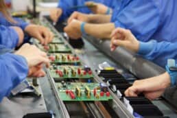
PCB ASSEMBLY TECHNOLOGIES
SURFACE MOUNT TECHNOLOGY
DOUBLE
THROUGH-HOLE TECHNOLOGY
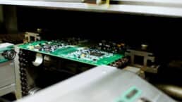
KEY STEPS IN THE PCB ASSEMBLY PROCESS
1. APPLY SOLDER PASTE
2. PLACE THE COMPONENTS
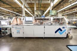
3. SOLDERING
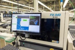
4. INSPECT THE ASSEMBLY
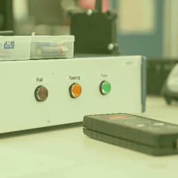
5. TESTING
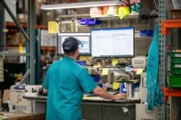
RIS PCBA EXPERTISE
About RiverSide Integrated Solutions
RIS is an advanced contract manufacturer providing robust solutions in circuit board assembly and product assembly. We employ more than 350 people and provide services to OEMs worldwide. We operate two state-of-the-art manufacturing facilities within the US.
With all of the choices in contract manufacturers out there, we know it can be challenging to find someone who understands your business model and has your best intentions in mind. RIS has always proven to be a win-win-focused relationship.
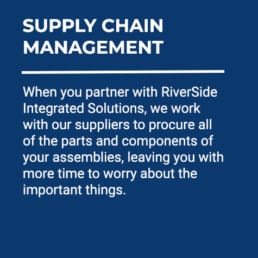
As your one-stop shop, we have the capabilities, capacity, quality assurance standards and resources to support all of your manufacturing needs. We understand that supply chain management is complex and very time-consuming, so we urge our customers to utilize us in the fullest capacity.
Our total-package solutions include:
- Extensive supply-chain network
- Full box-build assembly
- Dedicated Program Team
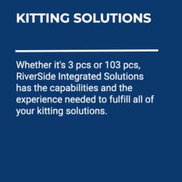
- Warehousing, kitting and drop-shipping capabilities
- Reverse logistics
- Flexible order fulfillment
- Scalability to meet your needs
Contact us today at (507) 523-3220 to see how we can help with your manufacturing project, or click contact us for a quote.
Get all of your manufacturing needs taken care
of at one company with these added value services.